When the pin level of the main control chip does not match the level of the external connected devices, a level conversion circuit is required for conversion. This is a problem that almost every electronic engineer will encounter. Today I will summarize several commonly used level conversion schemes, hoping to help you.
1. Use level conversion chip
This is probably the most stable, reliable and easy solution in all the solutions. Supply two power supplies on both sides of the conversion chip to be converted, and then connect the input and output signals to be converted on the input and output of the chip. All conversion parts are completed inside the chip. The following figure shows the bidirectional level converter.
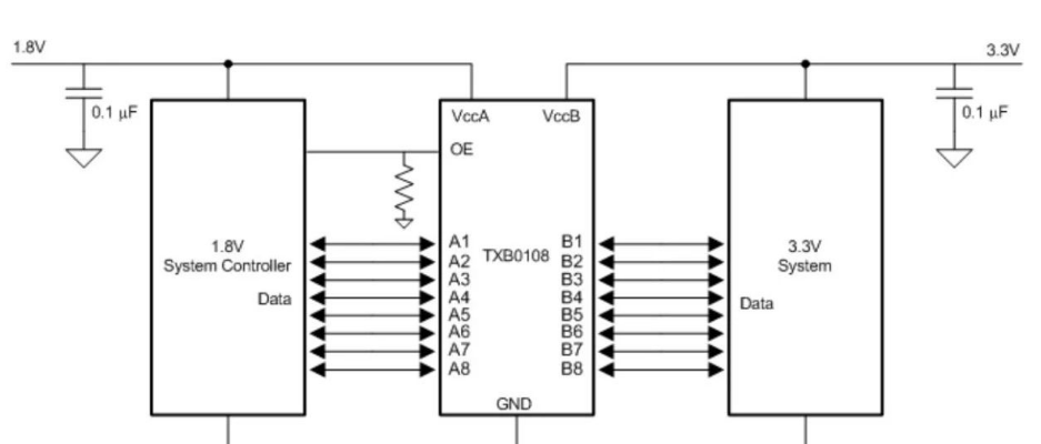
Of this scheme Many advantages The converter above can reach 100Mbps at most when the Vcca power supply voltage is above 2.5V, and the speed is very fast. In addition, it has the advantages of strong driving ability and simple use. of course There are also disadvantages The main reason is that there is no advantage in price, and it is difficult to use it in projects that need cost control.
2. Triode or MOS conversion level
This is a common scheme. It is recommended on the datasheet of the NB-IOT module I use. As shown in the figure below, when the TXD terminal is at the high level, the NPN triode is in the off state, and the RXD terminal is pulled up to its power supply voltage; When the TXD terminal is low, the NPN triode is on, and the RXD terminal is pulled down to the low level to complete the level conversion. The triode can also be replaced with MOS transistor.
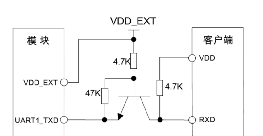
This scheme The biggest advantage Nothing is better than low cost, which is many times cheaper than the first scheme; Another is simple layout, which can be reasonably arranged according to the size of the circuit board. Disadvantages of this scheme It is also obvious that the speed is limited. The data in the datasheet mentioned above is not suitable for applications with a baud rate of more than 460800bps.
3. Use resistance voltage division to convert the level
This scheme should be the cheapest one. Only the resistor is used, as shown in the figure below. Let’s analyze this circuit. When the 3.3V level module sends data to the right side, it only passes through the current limiting resistor. When it reaches the right side, the level is within the receiving range of the client. When the 5V level client sends data to the left, the voltage is divided by two resistors, and the voltage of the left receiving terminal is 5V * 2K/(1K+2K) ≈ 3.3V.
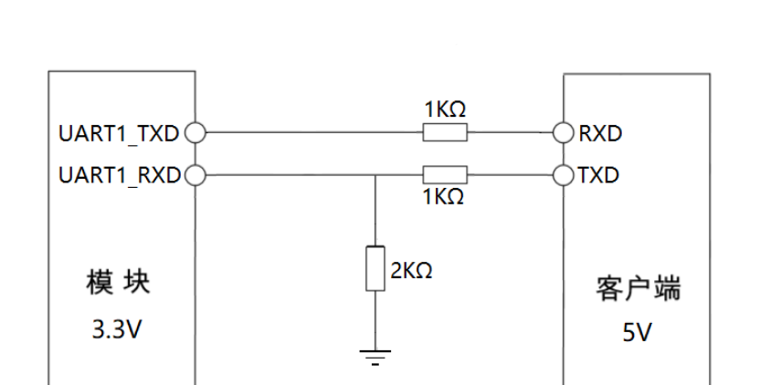
Advantages of this scheme It goes without saying that the cost is extremely low, only three small resistors are needed, and the layout is convenient, and the space on the PCB board is not occupied. of course The disadvantages are also great In order to reduce power consumption, the resistance value of the voltage divider should not be too small, which leads to weak driving ability and low speed, because of the influence of parasitic capacitance. Another is that there will be current crosstalk if there is no isolation at all.
4. Diode clamping conversion level
Diode clamping method is also a very common scheme to convert the level. The specific circuit is shown in the figure below. Let’s analyze this circuit. When the left TXD is low, due to the clamping effect of D2, the right RXD will get a low voltage equal to diode Vd; When the left TXD sends high level. Due to the clamping effect of D1, the right RXD will get a high level of 3.3V+diode Vd. The following group will better understand that when the right TXD sends a 5V high level, the left RXD receives a 3.3V+Vd level. Selecting a low-voltage drop Schottky diode can make the received level closer to 3.3V.
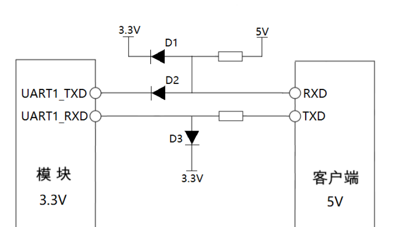
Advantages of this scheme It is cheap and easy to realize, and the leakage current is very small. Disadvantages through our above analysis You should already know that there is an error in the level. This error is the forward voltage drop of the diode, which may exceed the normal operating level of the chip; Another is speed. Because the existence of the current limiting resistor above will affect the speed, the speed can only be within 100K.
5. MOS tube and diode combination conversion level
This scheme was finally selected and used in the project after testing. As shown in the figure below. Let’s analyze that when the left TX is low, the right RXD is a forward voltage drop of 0.3V of 1N5819; When the left TX is high level 3.3V, the right RXD is pulled up to 1.8V. When the right TXD is low level, the NMOS tube is turned on, and the left RX is pulled to the low level; When the right TXD is high, the NMOS tube is cut off. The left RX is pulled to 3.3V.
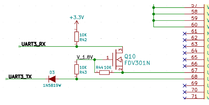
In fact, this scheme is very similar to the second scheme, so the advantages and disadvantages are similar. The advantages are low cost and strong driving ability. The disadvantage is that the speed cannot be too fast. My baud rate in the project is 115200bps, which is stable. I have never tried again.
summary
Let’s summarize several points that should be paid attention to when selecting the level conversion circuit: the most important is level matching, and the converted level should be within the acceptance range of the receiver; Another is the driving power after conversion; Another important point is the speed. If the converted waveform is distorted in the situation where the speed is required, it will lead to the inability to work; The last is cost, which is also critical.
