01 First“ impedance ”And“ impedance matching ”Concept of The resistance, capacitance and inductance existing in the circuit that hinder the current is called impedance. The unit of impedance is ohm (Ω) Z Is expressed as: Z=R+i(ωL–1/(ωC)) The plural of. real part R Is resistance, imaginary part (ωL–1/(ωC)) Is reactance, where ωL For inductive reactance, 1/(ωC) Is capacitive reactance.
One of the important parameters of earphones and speakers that we usually contact is impedance, which is exactly the impedance value of earphones in 1KHz sine wave signal circuit. Mainly resistance and inductive reactance, without capacitive reactance.
impedance matching It means that the signal source, transmission line and load achieve a suitable matching relationship, so as to improve energy efficiency.
02 Impedance matching in low frequency circuits
In the DC circuit, that is, the idealized pure resistance circuit, the reactance caused by capacitance and inductance can be basically ignored, and the impedance in the circuit is mainly from resistance.
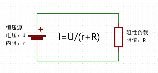
As shown in the following figure, we assume that the excitation source has been determined, then the load power is determined by the impedance matching degree of the two. Current in the circuit I =U/(r+R), load power P= I ² R, we collate P=(U ² * R)/(r+R) ², It can be seen that when R=r, the load power Pmax=U ²/4R.

This conclusion will be slightly different after the introduction of capacitive reactance and inductive reactance in the AC circuit Impedance conjugation The maximum power output can be achieved when In low-frequency circuits, we generally do not consider the matching of transmission lines, but only the impedance matching between the signal source and the load. Because the wavelength of low-frequency signals is very long relative to the transmission line, the transmission line can be regarded as a “short line”, and reflection can be ignored, because even if reflected back, it is the same as the original signal.
03 Impedance matching in high frequency circuits
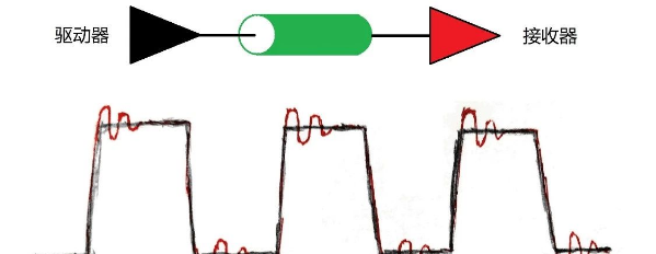
Why do I pull a single paragraph of high-frequency circuit? Because a very important factor is introduced into the high-frequency circuit – Reflected signal We know that when the signal frequency is very high, the wavelength of the signal is very short. When the wavelength and transmission line length are of the same order of magnitude, Reflected signal Superimposed on the original signal will change the shape of the original signal. However, if the characteristic impedance of the transmission line is equal to the load impedance (i.e. impedance matching), it will effectively reduce and eliminate high-frequency signal reflection.

As for the algorithm of reflection and characteristic impedance of transmission line caused by impedance mismatch, which involves the solution of second-order partial differential equation, I will not elaborate here. Interested friends can see the textbook Electromagnetic Fields and Electromagnetic Waves published by Higher Education Press, Chapter 7, Guided Electromagnetic Waves, Summary 6, Transmission Line, It has a detailed description.
We mentioned above Characteristic impedance of transmission line It is a very important concept. Its value is only determined by the structure and material of the transmission line, and has nothing to do with the length of the line and the frequency and amplitude of the signal. The characteristic impedance of the coaxial cable used by some RF equipment is 50 Ω, and the coaxial cable of closed-circuit television is generally 75 Ω.
What are the adverse consequences if the impedance does not match? In other words, the adverse consequences of reflection are mainly to reduce the energy transmission efficiency, form standing waves, and reduce the effective power capacity of the transmission line. If it is a RF device, it will affect the signal transmission distance, signal quality, and even damage the transmitting device. If the high-speed signal line on the circuit board does not match the load impedance, vibration and radiated interference may occur.
04 Application scenario of impedance matching
Design of RF antenna
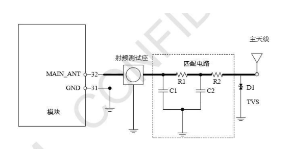
The key point of this is the impedance matching between the antenna and the feeder. When transmitting signals, the characteristic impedance of the transmitting antenna and the feeder shall be equal to obtain the best signal gain. When receiving signals, the antenna and the load should be conjugate matched. The receiver (load) impedance is generally considered to be only a real part, so it is necessary to use a matching network to remove the reactance part of the antenna and make their resistance parts equal. The following figure shows the datasheet of the antenna part of the NB IOT module of Simcom. The network analyzer is used to measure the impedance to determine the values of R1, R2, C1, C2, complete impedance matching, and achieve the best RF working state.
Terminal matching resistance
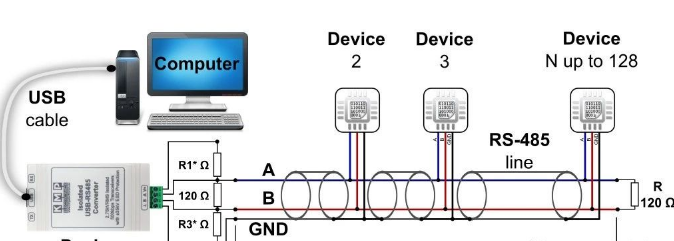
There is a detailed introduction in an article about 485 before us. Those who haven’t read it can read it. I believe that combining this article will have a deeper understanding. The characteristic impedance of twisted pair is generally 120 Ω. If no terminal resistance is added, the signal reflection mentioned above will easily occur when the cable length is very long and the transmission rate is high, that is, the signal frequency is high.

PCB wiring
In low-frequency circuit applications, impedance matching can be ignored, but in high-frequency circuit, the impedance of PCB wiring needs to be paid attention to. Generally, when the edge time of digital signal is less than 1ns or the frequency of analog signal exceeds 300MHz, we need to consider the impedance of wiring. PCB wiring impedance mainly comes from parasitic capacitance, resistance, inductance coefficient, and the main factors are plate thickness, line width, copper thickness and even via diameter. The range of PCB impedance is 25 to 120 ohms. USB, HDMI, SATA, etc. generally require 85 to 100 Ω impedance control. (The figure below shows the USB data cabling of a Linux minicomputer designed previously)
