01 Let’s start with the concept
The full English name of I2C is Inter Integrated Circuit, which literally means between integrated circuits, that is, what we often call the I-side C bus – I2C bus. It is a serial communication bus, which uses a multi master slave architecture. It was developed by Philips (the parent company of NXP) in the 1980s, and is used to connect motherboards and embedded systems to peripheral low-speed devices.
I2C is composed of two two-way open drain lines, which is a great advantage. The wiring is simple. The two wires use the pull-up resistance to pull up the potential. Typical potential is+3.3V or+5V. The standard transmission rate is 100Kb/s, and the low-speed mode is 10Kb/s.
02 physical layer
The figure below shows the physical topology of the I2C bus. As you can see, there are only two buses in total, one SDA (serial data) data line is used to carry data, and one SCL (serial clock line) clock line is used to control the timing of data transmission and reception. SDAs of all I2C devices are connected to SDAs of the bus, and SCLs are connected to SCLs of the bus. Each device has its own unique address to ensure the accuracy of access between devices.
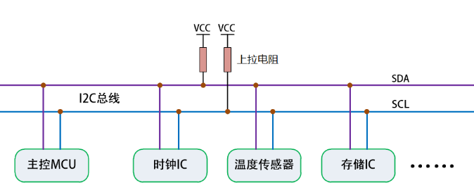
The connection of I2C in the physical layer can be said to be very simple, which is also its biggest advantage. The principle is to generate signals required by I2C bus protocol for data transmission by controlling the high and low level timing of SDA and SCL lines. When the bus is in the idle state, SCL and SDA are pulled up by the pull-up resistor and remain high.
It should be noted that the I2C communication mode is half duplex, because there is only one data line, and only one-way communication is possible at a certain time. This also shows that I2C is not suitable for large data transmission applications.
The difference between master and slave is very simple. The master issues the main command and the slave receives the command. The same I2C bus allows multiple masters.
03 protocol layer
As a basis, let’s first understand several important concepts.
1、 Initial state (i.e. idle state): the high level caused by the pull-up resistance of both SDA and SCL is the initial state;
2、 Start signal : When the SCL is high, SDA is pulled down, which is the start signal, indicating the start of communication.
3、 Termination signal : When SCL is high, SDA is pulled high, which is a termination signal, indicating that the communication is over.
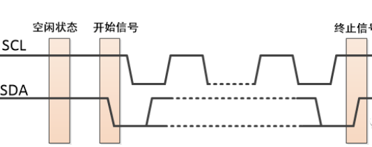
Did you find anything here? When the SCL is at a high level, the SDA level will be a signal once it changes, either starting or ending. So in During data transmission , When the SCL is at a high level, the SDA must remain stable. Only when the SCL is at a low level can the SDA change.
4、 Answer signal : After the transmitter has sent a byte/8-bit data to the receiver, the receiver must send a reply signal to the transmitter within the ninth clock cycle, so that the data transmission is successful. The high level meter does not respond, and the low level meter responds.


After we understand these signal states, let’s take a step by step look at how the data is transmitted.
1. Write a byte of data to a register of the slave device: start signal+device address (7 bits)+read/write (1 bit)+wait for slave response+register address (8 bits)+wait for slave response+data to be written (8 bits)+wait for slave response+stop signal. The following figure shows the sequence diagram of 24C02 EEPROM memory writing data.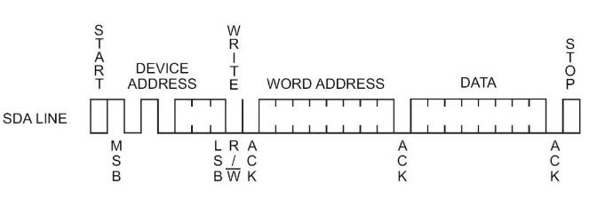
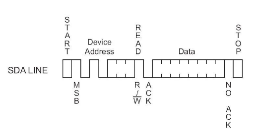
2. Let’s read it: the following figure shows the sequence diagram of reading a byte of data at the current address of 24C02. Is it clear at a glance. It is worth noting that when reading, the read/write status bit after the address 7 bits is 1. Here we will explain why there is NO ACK in the end. Under the “read” operation, the host is the receiver, and the NO ACK of the host means that the 24C02 data is stopped from being received, otherwise the 24C02 data will continue to be sent.
3. Let’s read a longer one: the following figure shows the sequence diagram of reading a byte of data at any address of 24C02. Start signal+equipment address (7 bits)+write (1 bit)+wait for slave response+data address (8 bits)+wait for slave response. The previous step is a fake write to tell 24C02 which address data to read. Continue, start signal+device address (7 bits)+read (1 bit)+wait for slave response+read data (8 bits)+wait for host (receiver) response+stop signal.

04 Make up dry goods
1、 Address of the device The address of I2C device is 8 bits, but the last bit during timing operation is not an address, but a read or write status bit. This is why the address of operations in the SH1106 library of arduino is not 0x7 – but 0x3 -. Because the first 7 bits are useful, the address is shifted one bit to the right as a whole. The first four digits of the address of another device are fixed, which is used by the manufacturer to indicate the device type. For example, the first four digits of the address of temperature sensor devices with I2C interface are generally 1001 (9X), the first four digits of the EEPROM memory address are generally 1010 (AX), and the first four digits of the oled screen address are generally 0111 (7X).
2、 The fatal disadvantage of I2C interface is that the transmission distance is close and the speed is slow 。 When you use the I2C bus interface, remember not to transmit in a long line, but only in the PCB board. Otherwise, occasionally losing data or even not reading data will make people crash. Don’t ask me how I know, but only tears.
3、 About why the two lines are designed as open drain As for this question, I remember that I foreshadowed you when I wrote “8 working modes of STM32 single chip I/O”. Let’s talk about the specific reasons today. There are two main points ① to prevent short circuit: if you think about that if you do not set it as open drain, but as push pull, several devices are connected to the same bus, then an IO output of one device is high, and an IO output of another device is low, then you will find that the VCC and GND of these two IO are short circuited; However, this problem will not occur if the leakage is opened, as shown in the following figure:

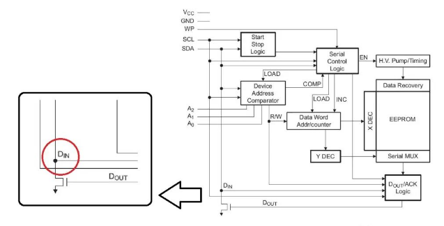
The second reason is “line and”. Let’s consider a scenario: if a device A on the bus pulls up the SDA, then another device B on the bus has pulled down the SDA. At this time, since 1&0=0, when device A checks the SDA, it will find that it is not high level but low level, which indicates that other devices on the bus have occupied the bus You have to give up. If the detection is high, you can use it. The following figure shows the internal diagram of 24C02 chip. You can see the status detection pin.
05 summary
As a common bus protocol, I2C bus is very worthy of our careful study. After we understand it, we can easily use any I2C interface device. I always think that in the process of learning, “being able to use” is not necessarily the end of our pursuit. When we can use it, we will gain unexpected joy by understanding something deeper.
